Research topics
Overview
The foundation of my research is the development of new, creative high-resolution methods for the nanoscale detection of electrical surface effects such as surface charges and dielectric properties. The aim is to understand the working mechanism behind functional nanostructures and interfaces, e.g. in perovskite solar cells or at solid-liquid interfaces. We recently started to collaborate with the biochemistry departemnt at JGU to investigate the structure of the membrane protein IM30 (left hand image in the tweet below). Ultimately, we plan to utilize the capabilities of electrical SFM modes to understand the role of electric and dielectric properties on nanoscale biosystems.
One day after #EventHorizon announced their picure of a #BlackHole, we finally managed to image a #protein ring using #AFM yesterday - there is a factor of ten sextillion (10^22) between the scalebars of those two images. pic.twitter.com/QLk6nAgMEV
— Stefan A.L. Weber (@StefanALWeber) April 12, 2019
Perovskite solar cells
The field of hybrid metal halide perovskites has skyrocketed in recent years. The reason is that with this new "wonder material", very efficient solar cells can be fabricated at very low material and manufacturing costs. The origins of the exceptional material properties can be found in the nano- and micrometer scale structure of the perovskite. So to study and finally understand the physics behind perovskite solar cells, force microscopy based methods are ideal. Our focus is on the development of new Kelvin probe force microscopy (KPFM) methods, e.g. to study the potential distribution in operating solar cell devices under illumination. Furthermore, we use Piezoresponse force microscopy (PFM) to investigate ferroic properties in perovskite thin films.
Hydrovoltaics and Solid-liquid interfaces
We recently discovered that water droplets sliding over an insulating hydrophobic surface charge up electrically. Given that nearly every surface in our lives comes in contact with water, this water-dependent surface charging (“hydrovoltaic effect”) may be a ubiquitous process. We are investigating this phenomenon within the ERC Advanced Grant Dynamic charging at moving contact lines of Prof. Hans-Jürgen Butt.
Next to developing new methods for studying hydrovoltaic effects, we are interested in mapping and understanding molecular effects directly at solid liquid interfaces. Our homebuilt low-noise SFM setup allows topography mapping with molecular and atomic resolution. In addition, we want to develop new methods to quantify and map the molecular interactions in liquid media. In particular, we want to quantify the electrostatic contributions by developing new Kelvin probe force microscopy methods adapted for the use in liquid electrolytes.
Methods
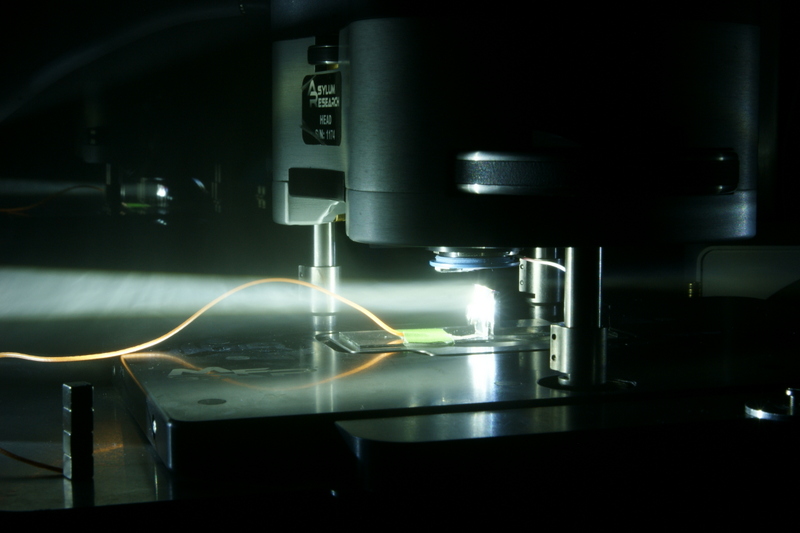
Low-noise force microscopy
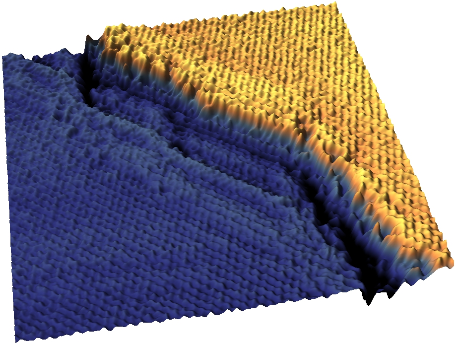
In order to image the surface with the highest possible resolution, dynamic operation modes using a vibrating tip are preferable. Here, the cantilever resonance and lock-in detection can be used to boost the signal-to-noise ratio. Under ambient conditions, the SFM has to be operated at high mechanical amplitudes of several tens of nanometers to maintain a stable oscillation. At lower amplitudes, capillary forces due to water and hydrocarbon adsorbates on the sample surface make the tip stick to the surface and the oscillation breaks down. For measurements in air, noise is less important as the signals are large. On the other hand, the tip stays in close proximity to the sample surface only for a very short time when the tip "tapps" on the surface. Thereby, the lateral resolution is limited to the tip radius and atomic resolution is mostly impossible. In liquid environments it is possible to operate the SFM with very small mechanical amplitudes, often less than a nanometer. Here, the tip stays within the interaction region close to the surface. If the noise level in the cantilever deflection signal is low enough, atomic resolution can be readily obtained.
One example for the high resolution capabilities of SFM in liquids is the image above. It shows an atomically resolved stepedge on graphite. This image was recorded in the very viscous environment of a glycerol-water mixture.
In our group we have developed a low-noise SFM setup that minimizes the influence of the detection noise. At the same time, this device allows a fast implementation of new measurement modes, as all the raw signals can easily be fed in and read out of the SFM. This device is currently our workhorse for the development and testing of new SFM methods.
Kelvin probe force microscopy
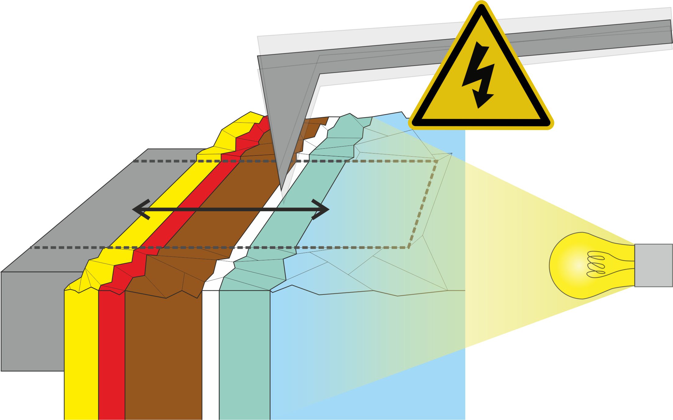
Kelvin probe force microscopy (KPFM) is a SFM adaptation of an old method to measure contact potentials developed by Lord Kelvin. Here, the key feature is that KPFM can quantify and decouple electrostatic interactions from other forces between a SFM tip and a sample. The idea is to enhance electrostatic forces by additionally applying a voltage between a conductive nanoscale tip and the sample surface. In KPFM, an alternating voltage VAC is applied and the response tracked by means of a lock-in amplifier. By applying an additional DC voltage VDC to the tip, the electrostatic force can be minimized if VDC = VCPD, where VCPD is the contact potential difference between the tip and the sample. The tracking of VCPD is usually done by a feedback (closed loop operation). For the application in liquid electrolytes, we are using and developing new open loop KPFM methods that do not require DC voltages.
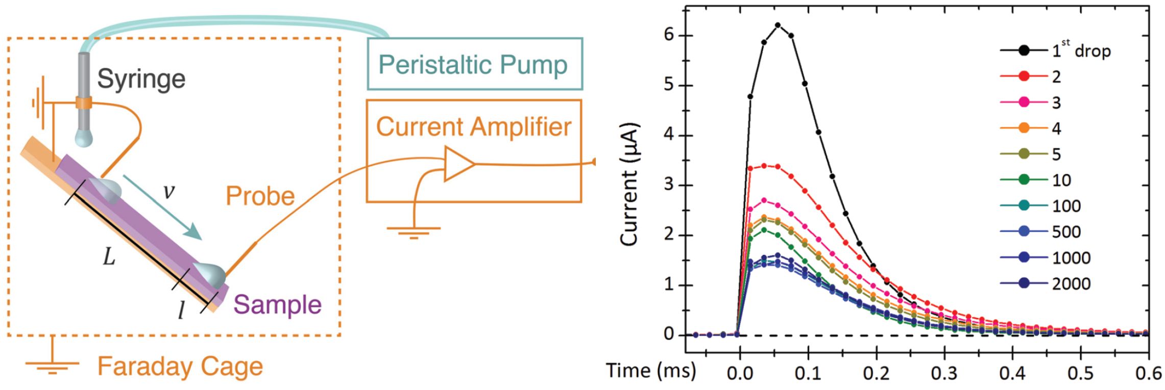
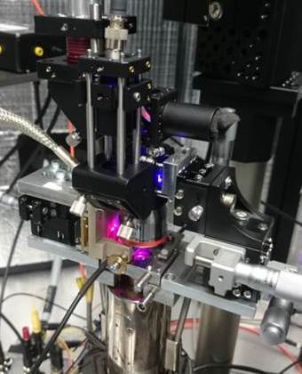
For the investigation of Perovskite solar cells, we have developed a method to study device cross sections of solar cells. Thereby the cross section is exposed by cleaving the device in half. Subsequently, the cross section is polished by a focused ion beam to obtain a roughness lower than 10-50 nm. This step is important to avoid cross talk between the topography and the measured surface potential. By using a platinum protection layer, we can avoid ion contamination of the active layer.
Recently, we have extended the capabilities of KPFM to measure the dynamics of the charge distribution. Usually, we scan the tip line by line across the sample. This is very slow: roughly a second per scanline, 5-15 minutes per image. To make KPFM faster, we developed a time-resolved KPFM method, where we record the response of the cell to a light or voltage pulse point by point. Thus, we can reconstruct complete KPFM maps with a temporal resolution of 500 µs.
Piezoresponse force microscopy
Piezoresponse force microscopy (PFM) images electromechanical properties of ferroelectric samples via the inverse piezoelectric effect: By applying a voltage to a ferroelectric material, the compound expands or contracts depending on the orientation of its internal polarization. In PFM, an AC voltage is applied to the sample via a conductive tip in contact scanning mode. Consequently, the sample responds by oscillating mechanically. The phase lag between the AC excitation and sample’s piezoresponse depends on the local orientation of the polarization. For ferroelectric domains with a polarization perpendicular to the surface, the piezoresponse phase changes by 180° on oppositely oriented domains. The amplitude of the piezoresponse depends on the excitation amplitude and the sample’s piezoelectric coefficient, which gives the magnitude of the electromechanical coupling. At the domain boundary between two oppositely oriented domains the piezoresponse of both domains cancel out and the PFM amplitude becomes zero.
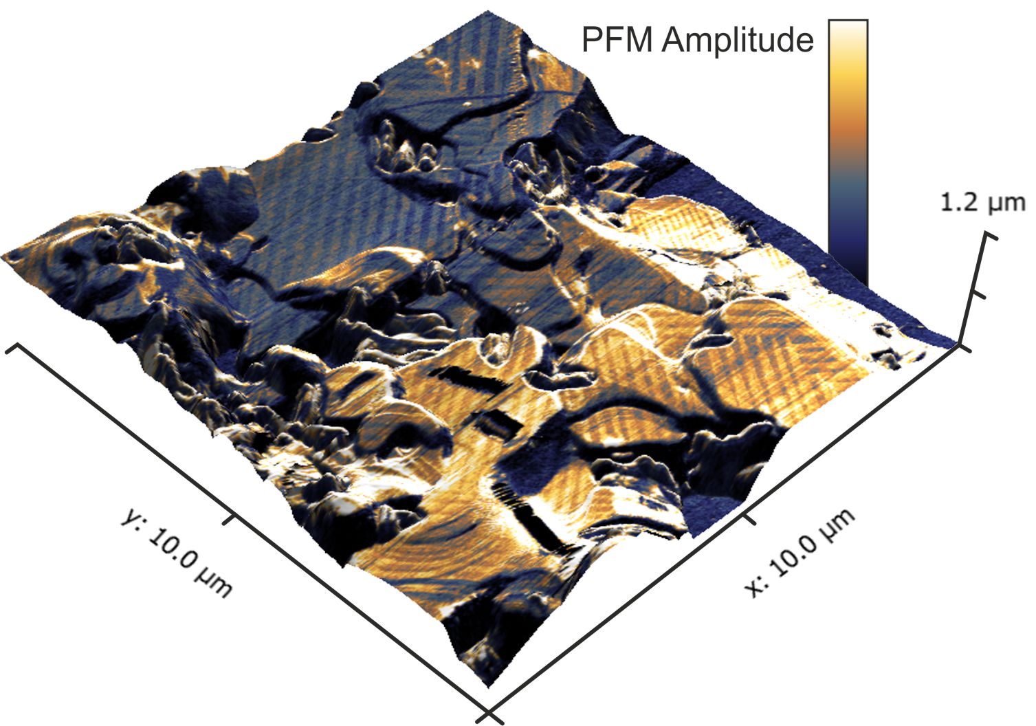
In our PFM study on hybrid perovskite thin films, we observed a distinct periodic pattern in the piezoresponse of methylammonium lead iodide perovskite not correlated to any topographic features. The origin of this pattern is connected to so-called ferroelastic twin domains that form during the cubic-tetragonal phase transition to release internal strain in the crystallites. We recently found that the electronic charge carrier diffusion is almost 60% faster in directions parallel to the domains compared to perpendicular directions.
Here, you can listen to the paper, read to you by the author: